30 industrials and 50 students gathered in October at AP Hogeschool in Antwerp for the event “Connect! ‘Printed electronics’ as a motor for IoT. A full-day program was waiting for them with all actors from the world of printed electronics: material suppliers, researchers and production companies.
In the introduction, the event-organizers indicated how they view these new developments. Fons Put (VIGC) listed the suitability of printing processes for the production of new technologies: top effciency (minimum material consumption), suitable for flexible materials (paper and plastics), various printing technologies available and backed up with an extended recycling chain. Geert Vanhulle (Lecturer Electronics-ICT at the AP Hogeschool Antwerpen) sketched a nice historical overview of the production of PCB’s (printed circuit boards). An evolution from rigid materials with cumbersome connectors to the new generation of flexible structures.
The first speaker session focused on suppliers of inks and adhesives for functional printing. Bavo Muys, Application Manager of Printable Electronics at AGFA Materials, clearly described the pros and cons of the two types of ink that AGFA offers: a transparent electrically conductive polymer ink (PEDOT: PSS) and a nano-silver ink with superfine silver particles. An important application market lies in the household appliances and automotive industry (capacitive switches). Furthermore, a nice bridge was built with graphic knowledge: how can a line pattern with silver ink be printed to become invisible?
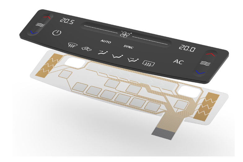
Fig.1. A printed structure for automotive touch application (Quad Industries)
Inge van der Meulen, Product Development Manager Electronic Printing at Henkel Belgium, showed how printed electronics are interwoven in the large product range of Henkel. The Henkel portfolio includes a number of large Brands (including Persil, Schwarzkopf), and Henkel is the market leader in adhesives products for industrial applications. In doing so, they strongly anticipate the trend of hybrid electronics: printed conductor tracks in combination with applied powerful silicon-based components. In addition to classic soldering materials, current-conducting adhesives have been developed.
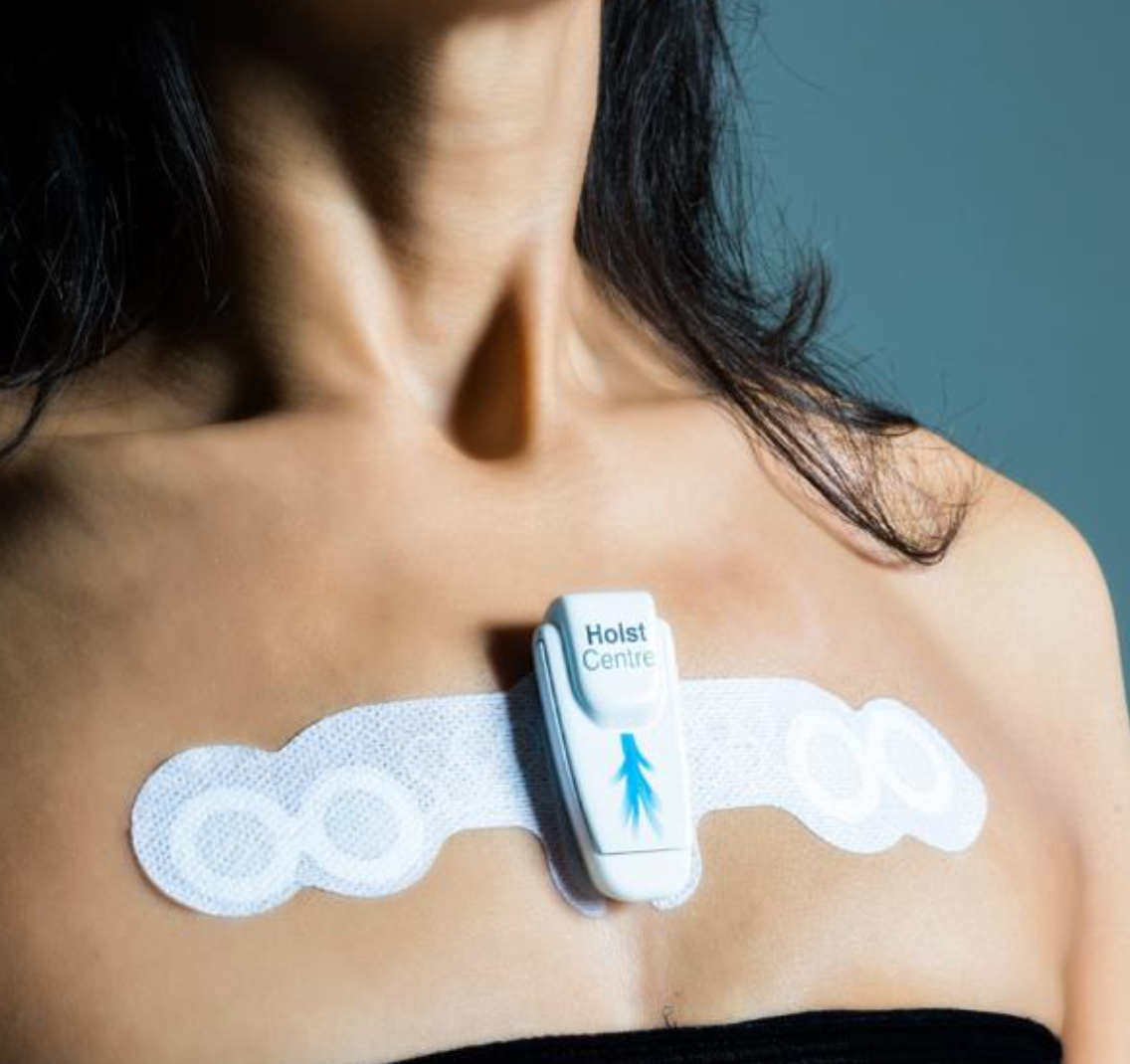
Fig. 2. A printed medical sensor.
Marcel Klok is Sales Director for Asia and Head of Procurement, Business Development and Innovation at Dutch Royal Koninklijke Joh. Enschedé. As a former financial printer, the company is specialized in security, which Marcel immediately demonstrated by hacking the integrated NFC from the program booklet. Marcel explained his way of doing business: new concepts are discussed and evaluated in a worldwide network. After a ‘Go’, it’s time for action and within a few months first realisations have to be there. This approach was illustrated with the acquisition of AntTail. A total concept has been developed for parcel shipping, that is currently being rolled out in Finland.
After the coffee break representatives of research centers entered the stage The kickoff was given by Dr. Kris Myny, Principal Member of Technical Staff / R & D Team leader at imec. Kris is a pioneer in chip production on flexible film with the fully flexible RFID / NFC as one of his expertise. Within the Met@-link project an NFC tag was produced with screen-printed antenna and integrated flexible tag.

Fig. 3. The first printed flexible CPU, 40 years after the silicon chip (with the same specs!).
Auke Jisk Kronemeijer is a Senior Researcher working at the Holst Center / TNO on printed displays. The aspect of integrating new technology into existing production processes is a nice exponent of pragmatic thinking. Flat-panel TVs are now produced on a large glass plate. By using this in the new flexible technology as a substrate on which the functional layers are printed, the ‘old’ production method can still be used. A point of attention is a delamination step, in which the flexible display is removed from the glass substrate.
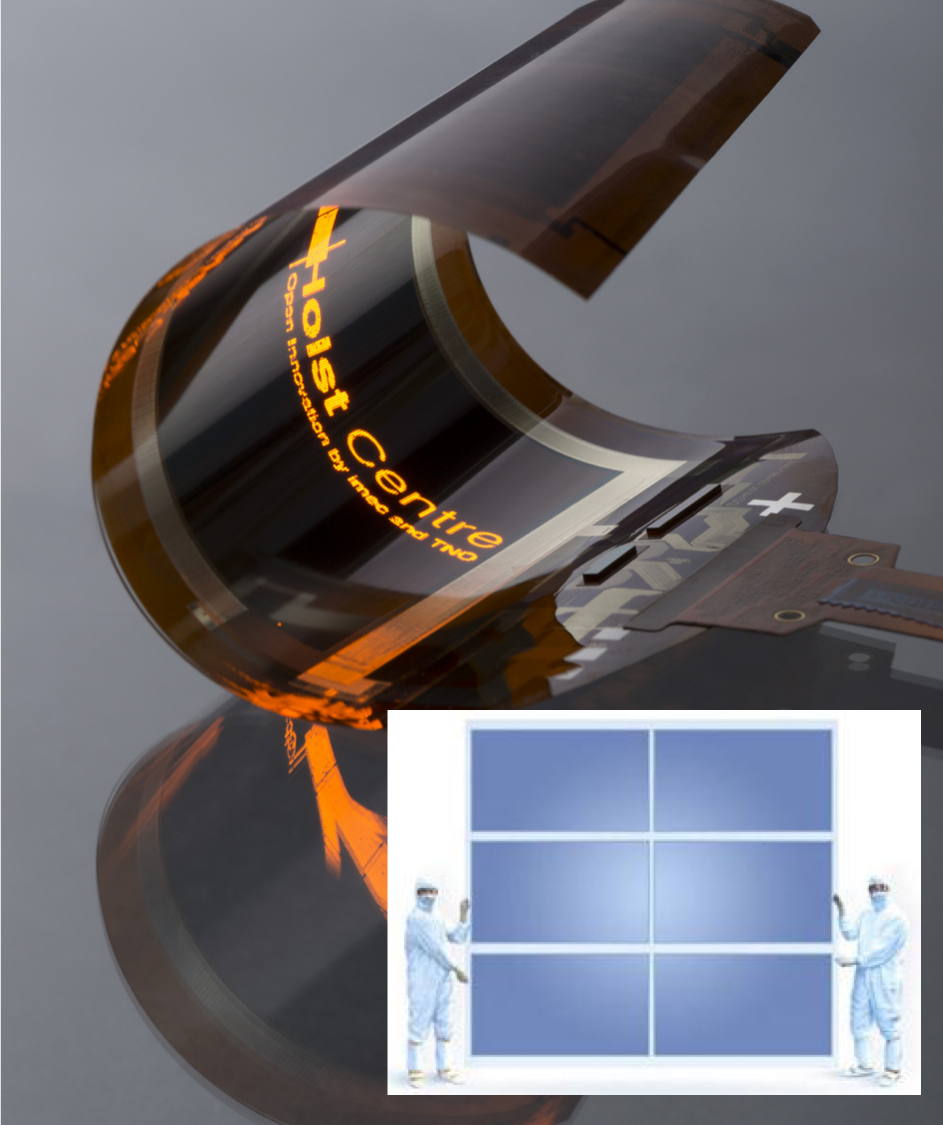
Fig. 4. A flexible display next to the classic flat panel production on large glass plates.
In the IMO / IMOMEC labs at the University of Hasselt, Wim Deferme has gained considerable experience with various printing techniques with conductive and functional inks. In addition to screen printing and inkjet, this includes printing techniques such as ultrasonic spray coating and spin coating. Wim is active in the Acpel project in which luminescent (illuminated) structures are screen printed on a textile carrier: stretchable but still functioning. In addition, numerous new printing concepts were reviewed: Bio-impedance sensor, moisture detector, PH sensor, printed heating element, 3D electroprint. The University of Hasselt is the driving force behind the new Paperonics project. In this project applications with functional inks on paper and cardboard are being developed.
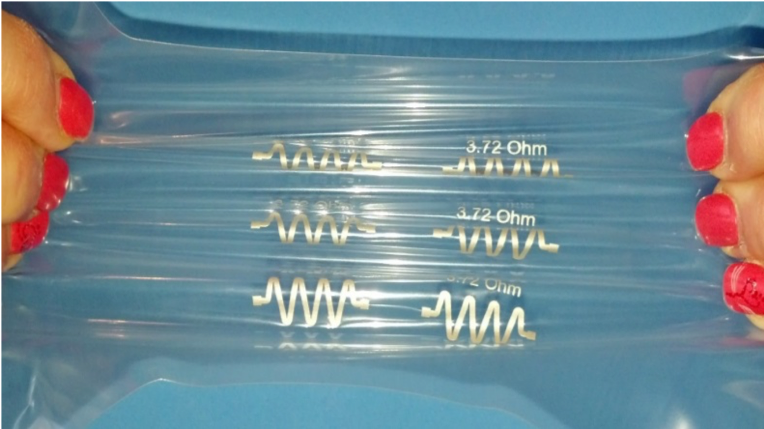
Fig. 5. In a number of applications your printed conductor needs to be stretchable.
After the research centers the stage was given to the production companies. Kristof Baes is process engineer at Quad Industries. Quad industries produces hybrid electronics on an industrial scale: screen printing of conductors, assembly of components, adhesive bonding, and cutting. A selection from their range of new products:
- Touch film for the automotive industry to replace the classic dashboard.
- Capacitive sensors, including a rollable chessboard with which you can play against a virtual opponent.
- 3D shaped electronics, including a 3D touch wheel, very useful for hospitals (fully encapsulated and easy to disinfect).
- Smart packaging, including a temperature logger
- Project ARION, thin shoe inlays to measure load when walking.
- Smart blister with a NPS-communicating skin patch

FIG. 6. 3D-touch wheel from Quad Industries.
“Who is going to press the button”? This was the opening quote from Hans van de Mortel to illustrate the challenge for the production companies. Hans is the owner of Metafas, producer of printed electronics. They can illuminate superfine silkscreen structures with their laser-guided illuminator, with which high-quality conductive patterns can be printed. The research work of the knowledge centers leads to a considerable stream of new concepts. Converting these to the market, however, is another thing. The leading actors have to take the next step as illustrated by the ‘smart blister’. Everyone is convinced of the concept: accurate registration and dosing of the intake of medicines will help both patient and doctor. But in order to achieve this, all actors in the field (pharmaceutical industry, medicine, health inspection, …) have to reach an agreement. This takes lots of time and effort.
Closing speaker of the event was Steven Sanders, owner of Quicksand. Quicksand designs microelectronics with expertise in the optimization of energy consumption and wireless communication. Amongst their successful electronics designs, we find the ZembrO. This is a portable device that communicates the position and movement of the elderly to allow them to live longer in their own homes. The collaboration with bloom technologies is also successful. This resulted in the design of a smart patch to monitor the pregnancy. With this, the Branson Extreme Tech Challenge was won in 2016. Steven explained the Internet- of-things strategy. In 2020 more than 50 billion connected devices are expected. Basic question is which communication technology does fit this concept best? 4G / 5G networks are built to obtain as much bandwidth as possible. For communications with Internet-of-things devices different objectives can play a role, such as energy consumption and cost price. A smart water meter sends 2X daily its consumption: it is not the bandwidth but energy consumption that is important (the sensor must be capable to report autonomous for 16 years). The three largest networks for such applications are ‘Lora’, ‘NB-IoT’ and ‘Sigfox’.
Interesting links provided by the speakers:
Inge van der Meulen, Henkel Belgium
https://www.henkel.com/brands-and-businesses/adhesive-technologies
https://www.henkel-adhesives.com/us/en/industries/electronics.html
Marcel Klok & Jan-Peter van Dok, Koninklijke Joh. Enschedé
https://www.joh-enschede.nl/#homegallery
Wim Deferme, Faculty of Industrial Engineering Sciences Imo-Imomec – Functional Materials Engineering
https://www.youtube.com/watch?v=cM10uk1EPEA
https://www.youtube.com/watch?v=kXmKRROzvks
https://www.youtube.com/watch?v=sRUix7BHCTY
https://www.3delektroprint.be/
Kristof Baes, Quad Industries
https://www.quad-ind.com/printed-electronics/
https://www.quad-ind.com/quad-industries-and-invisible-jointly-demonstrate-electrochromic-printing-onto-nfc-rfid-tags/
https://www.quad-ind.com/pressure-sensitive-insole-tracks-every-movement-of-your-foot/
https://www.quad-ind.com/user-interfaces/capacitive-touch/